八核心單片機(jī)有什么優(yōu)點(diǎn)
FPPA 架構(gòu)介紹
FPPA 產(chǎn)品特色
內(nèi)建硬體的即時(shí)作業(yè)系統(tǒng)
FPPA 暫存器說明
FPPA 軟體規(guī)劃
FPPA 指令介紹

八核心平行處理單片機(jī) (FPPA) 介紹
八核心單片機(jī)有什么優(yōu)點(diǎn):
相信許多研發(fā)人員都有選擇 MCU 的痛苦經(jīng)驗(yàn), 選這顆 MCU 少個(gè) UART,選那顆 Timer 又不夠,就算選好了 MCU,寫多功 (Muti-Task)的軟體才是真正痛苦的開始.
應(yīng)廣科技(Padauk )八核心平行處理單片機(jī)Field Programmable Processor Array, 以下簡稱“FPPA”,利用八核心平行處理可一次解決軟體“Muti-Task” ,“Timer” 和MCU 所需的各種周邊的困擾.有八顆MCU 平行處理,不用再煩惱多工軟體,有八顆MCU 平行處理等于有八個(gè)Timer,不用再煩惱Timer 不夠,有八顆MCU 平行處理,拿幾顆來寫UART,I2C,SPI ,PWM 等周邊就不用再煩惱介面不夠.
FPPA 架構(gòu)介紹

如上圖所示
基本上應(yīng)廣科技(Padauk )的FPPA, inside 了8 顆RISC type 1T 的MCU, 除了每顆MCU 有自己的Flag ,PC counter, Stack pointer, Accumulator 外,其余的ROM,RAM,IO 等是共用的.故每一MCU 都可隨時(shí)監(jiān)控其他MCU 的狀況.(MCU#0 還多了16bit 的timer & 中斷管理可處理I/O中斷和內(nèi)部中斷).
8 顆MCU 是平行處理,且每個(gè)I/O 都可設(shè)為input 或output 或pull-hi 或open-drain,故可用軟體去控制I/O寫各種周邊介面, 如I2C, UART,PWM,SPI等非常有彈性(如MCU#0 寫UART, MCU#1寫I2C, MCU#2 寫PWM 等,幾乎沒有限制.) 軟體去作SOC 周邊功能,故成本很有競爭力,和彈性,不會(huì)受限一般MCU 原廠所開的IC 規(guī)格.
除了 一般 MCU 的指令外, 還有 類似 FPGA 才有 I/O 指令,對(duì) I/O 的處理特別精簡和有效率.可取代部分的 PAL/GAL/FPAG 等邏輯合成電路.
產(chǎn)品特色 Features
內(nèi)建 8 顆 RISC type 平行處理,多核心 CPU 矩陣 (Field Programmable Processor Array“FPPA”).
內(nèi)建硬體的即時(shí)作業(yè)系統(tǒng) (hardware RTOS).
97 個(gè) 1T RISC type 功能強(qiáng)大的指令. (不同系列,指令略有增減)
支援 C/Assembly language/Macro 程式語言.
可自由規(guī)劃每一 MCU 的堆疊(stack pointer) 深度.
支援12bitx8ch ADC.
彈性方便的位元操作指令 (Bit-manipulation).
全部的資料記憶體都可用指標(biāo)定址 (index pointer addressing).
可自由規(guī)劃每一 MCU 的程式空間 ( OTP program memory).
每一 I/O 都可彈性定義為 input 或 output或 pull-hi或 open-drain.
內(nèi)建高速/慢速 RC振蕩器.
獨(dú)家的 intra-FPP handshaking指令,每一 MCU 可控制其他 MCU 的程式指標(biāo) (program counter).
獨(dú)家的內(nèi)部中斷,MCU#1 – MCU7 可發(fā)出中斷需求,讓 MCU#0當(dāng)中斷優(yōu)先處理.
獨(dú)家的 “wait0”, “wait1” 指令,對(duì) IO 的處理特別精簡和有效率.
獨(dú)家的 “delay x” (x 0 – 255)指令,可直接 delay x 的 system clock.
內(nèi)建硬體的即時(shí)作業(yè)系統(tǒng) (hardware RTOS)
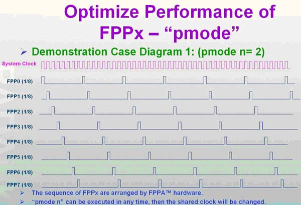
FPPA 最多可有8 顆MCU 同時(shí)平行處理, FPPA 有一“pmode”指令可調(diào)整每一MCU 的速度,FPPA 根據(jù)“pmode”由硬體強(qiáng)制去分配的每一MCU 的bandwidth 來完成類似軟體RTOS 的功能(如下表),完全不用寫軟體的RTOS.
| pmode | FPP0 | FPP1 | FPP2 | FPP3 | FPP4 | FPP5 | FPP6 | FPP7 |
| 0 | 1/2 | 1/8 | 1/16 | 1/16 | 1/16 | 1/16 | 1/16 | 1/16 |
| 1 | 1/4 | 1/4 | 1/8 | 1/8 | 1/16 | 1/16 | 1/16 | 1/16 |
| 2 | 1/8 | 1/8 | 1/8 | 1/8 | 1/8 | 1/8 | 1/8 | 1/8 |
| 3 | 1/2 | 1/8 | 1/8 | 1/8 | ||||
| 4 | 1/4 | 1/4 | 1/4 | 1/8 | 1/8 | |||
| 5 | 1/16 | 1/4 | 1/4 | 1/4 | 1/16 | 1/16 | 1/16 | |
| 6 | 1/16 | 1/2 | 1/8 | 1/16 | 1/16 | 1/16 | 1/16 | 1/16 |
| 7 | 1/8 | 1/2 | 1/8 | 1/8 | 1/8 |
如下圖為 pmode =2 , 平均每一 MCU 分配 1/8 system clock
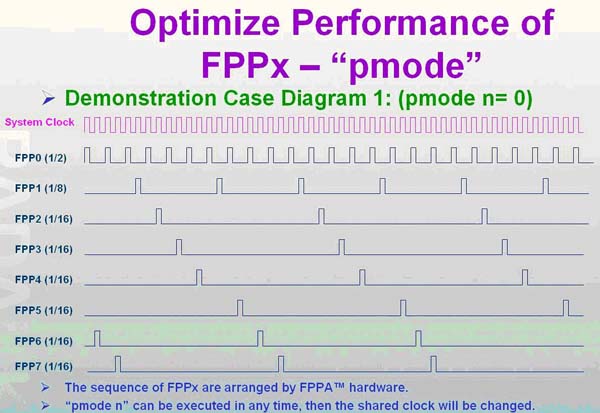
下圖為 pmode=0 ,FPP#0 = 1/2 system clock, FPP#1 = 1/4 system clock, FPP#2-FPP#7 = 1/16 system clock ,每個(gè) FPP 的 cycle 如下
FPPA暫存器 (Registers) 說明
| Name | Address | Function |
| flag | 0x00 | Arithmetic status flag |
| fppen | 0x01 | FPP unit enable register |
| sp | 0x02 | Stack pointer |
| clkmd | 0x03 | Clock mode register |
| inten | 0x04 | Interrupt enable register |
| intrq | 0x05 | Interrupt request register |
| t16m | 0x06 | Timer 16 mode register |
| gdio | 0x07 | General data register for IO |
| mulop | 0x08 | One operand for multiplication |
| mulrh | 0x09 | High byte result of multiplication (read only) |
| eoscr | 0x0a | External oscillator setting register |
| ihrcrl | 0x0b | Internal high RC oscillator control register low |
| Ihrcrh | 0x0c | Internal high RC oscillator control register high |
| pa | 0x10 | Port A data register |
| pac | 0x11 | Port A control register |
| paph | 0x12 | Port A pull high register |
| paod | 0x13 | Port A open drain register |
| pb | 0x14 | Port B data register |
| pbc | 0x15 | Port B control register |
| pbph | 0x16 | Port B pull high register |
| pbod | 0x17 | Port B open drain register |
| pc | 0x18 | Port C data register |
| pcc | 0x19 | Port C control register |
| pcph | 0x1a | Port C pull high register |
| pcod | 0x1b | Port C open drain register |
| pd | 0x1c | Port D data register |
| pdc | 0x1d | Port D control register |
| pdph | 0x1e | Port D pull high register |
| pdod | 0x1f | Port D open drain register |
| pe | 0x30 | Port E data register |
| pec | 0x31 | Port E control register |
| peph | 0x32 | Port E pull high register |
| peod | 0x33 | Port E open drain register |
PPA 共有33 個(gè)暫存器(不同系列暫存器略有不同),其中address 0x10 – 0x32 各為I/O Port A – Port E 的控制暫存器,故真正要注意的register 只有13 個(gè),不像其他MCU,周邊控制(如PWM,I2C,UART 等)的register 就好幾拾個(gè),故FPPA 很容易學(xué)習(xí)U. 13個(gè)register 中比較容易引起誤解,或datasheet 描述不易理解的地方特別提出說明.
“sp” & “flag”: 由于 FPPA 有8顆 MCU,故每一 MCU 看到的 “sp” & “flag” 的值是不一樣的值.
“fppen”: 由于 FPPA 有8顆 MCU,但并不是每個(gè)應(yīng)用 8 顆 MCU 都要去 enable, 故可用 “fppen” register 去控制那些 MCU 需要 enable.
gdio”: register “gdio” 可以做下列二種應(yīng)用
當(dāng)warm-boot 或cool-boot的判斷用:由于FPPA 開機(jī)或reset 時(shí), “gdio” 的值不會(huì)去變更,故程式執(zhí)行中可故意寫入一個(gè)值給“gdio”,而在程式開始的地方去判斷“gdio” 的值是否為程式執(zhí)行中所寫入的值即可判斷MCU 是否是第一次開機(jī)或是reset 再開機(jī).
讓MCU & MCU 間的溝通更有效率:“wait0” 和“ wait1” 指令除了可對(duì)I/O 處理外, 也可對(duì)“gdio” 暫存器處理, (Ex.: “wait0 gdio.x”) , 例如在MCU#1 中把“gdio.x” 設(shè)為0 或1, MCU#2 用“wait0” 或“wait1”指令去做條件的判斷亦可達(dá)到MCU#1 和MCU#2 之間的溝通.
FPPA 軟體規(guī)劃
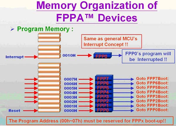
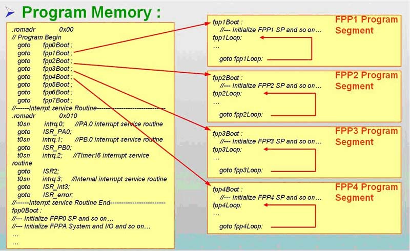
如上圖所示,和大多數(shù)的MCU 一樣,FPPA 也有所謂“中斷向量表”的概念,只是一般MCU 的中斷向量是“中斷副程式” 的進(jìn)入位置,FPPA 的中斷向量是各FPP 的進(jìn)入位置.如上圖中address 0h-7h 分別為FPP#0-7 的進(jìn)入位置,address 0x10 才是“中斷副程式” 的進(jìn)入位置,故其程式寫法如下
FPPA 指令介紹 (Instructions Set)
| FPPA Instructions Set | |
| Data Transfer Instructions (16) | |
| Instruction | Function |
| mov a,I | Move immediate data to ACC。 |
| mov M,a | Move data from ACC to memory |
| mov a,M | Move data from memory to ACC |
| mov a,IO | Move data from IO to ACC |
| mov IO,a | Move data from ACC to IO |
| pushw index | Move the content of index to be the content of stack pointer |
| pushw pcN | Move the content of program counter of Nth FPP unit to be the content of stack pointer |
| popw index | Restore the content of stack pointer to be the content of index |
| popw pcN | Restore the content of stack pointer to be the content of program counter of the Nth FPP unit |
| ldtabh index | Load high byte data in OPT to ACC by using index as OPT address |
| ldtabl index | Load low byte data in OTP to ACC by using index as OTP address |
| ldt16 index | Move 16-bit counting values in Timer16 to memory which is addressed by index |
| stt16 index | Store 16-bit data from memory addressed by index to Timer16 |
| idxm a,index | Move data from specified memory to ACC by indirect method |
| idxm index,a | Move data ACC to specified memory by indirect method |
| xch M | Exchange data between ACC and memory |
| Arithmetic Operation Instructin (20) | |
| add a,I | Add immediate data with ACC, then put result in ACC |
| add a,M | Add data in memory with ACC, then put result in ACC |
| add M,a | Add data in memory with ACC, then put result in ACC |
| addc a,M | Add data in memory with ACC and carry bit, then put result in ACC |
| addc M,a | Add data in memory with ACC and carry bit, then put result in memory |
| addc a | Add carry with ACC, then put result in ACC |
| addc M | Add carry with memory, then put result in memory |
| nadd a,M | Add negative logic (2's complement) of ACC with memory |
| nadd M,a | Add negative logic (2's complement) of memory with ACC |
| sub A,I | Subtraction immediate data from ACC, then put result in ACC. |
| sub a,M | Subtraction data in memory from ACC, then put result in ACC. |
| sub M,a | Subtraction data in ACC from memory, then put result in memory |
| subc a,M | Subtraction data in memory and carry from ACC, then put result in ACC |
| subc M,a | Subtraction ACC and carry bit from memory, then put result in memory |
| subc a | Subtraction carry from ACC, then put result in ACC |
| subc M | Subtraction carry from the content of memory, then put result in memory |
| inc M | increment the content of memory |
| dec M | Decrement the content of memory |
| clear M | Clear the content of memory |
| mul | Multiplication operation. An 8x8 unsigned multiplication will be executed. |
| Shift Operation Instructions (11) | |
| sr a | Shift right of ACC |
| src a | Shift right of ACC with carry |
| sr M | Shift right the content of memory |
| src M | Shift right of memory with carry |
| sl a | Shift left of ACC |
| slc a | shift left of ACC with carry |
| sl M | Shift left of memory |
| slc M | Shift left of memory with carry |
| swap a | Swap the high nibble and low nibble of ACC |
| swap M | Swap th high nibble and low nibble of memory |
| Logic Operation Instructions (16) | |
| and a,I | Per logic AND on ACC and immediate data, then put result in ACC |
| and A,M | Per logic AND on ACC and memory, then put result in ACC |
| and M,a | Per logic AND on ACC and memory, then put result in memory |
| or a,I | Per logic OR on ACC and immediate data, then put result in ACC |
| or a,M | Per logic OR on ACC and memory, then put result in ACC |
| or M,a | Per logic OR on ACC and memory, then put result in memory |
| xor a,I | Per logic XOR on ACC and immediate data, then put result in ACC |
| xor a,M | Per logic XOR on ACC and memory, then put result in ACC |
| xor M,a | Per logic XOR on ACC and memory, then put result in memory |
| not a | Per 1's complement (logical complement) of ACC |
| not Mry | Per 1's complement (logical complement) of memo |
| neg a | Per 2's complement of ACC |
| neg M | Per 2's complement of memory |
| comp a,I | Compare ACC with immediate data |
| comp a,M | Compare ACC with the content of memory |
| comp M,a | Compare ACC with the content of memory |
| Operation Instructions (6) | |
| set0 IO.n | Set bit n of IO port to low |
| set1 IO.n | Set bit n of IO port to high |
| tog IO.n | Toggle bit state of bit n of IO port |
| set0 M.n | Set bit n of memory to low |
| set1 M.n | Set bit n of memory to high |
| swapc IO.n | Swap the n-th bit of IO port with carry bit |
| Conditonal Operation Instructions (13) | |
| ceqsn a,I | Compare ACC with immediate data and skip next instruction if both are equal |
| ceqsn a,M | Compare ACC with memory and skip next instruction if both are equal |
| cesn M,a | Compare ACC with memory and skip next instruction if both are equal |
| t0sn IO.n | Check IO bit and skip next instruction if it's low |
| t1sn IO.n | Check IO bit and skip next instruction if it's high |
| t0sn M,n | Check memory bit and skip next instruction if it's low |
| t1sn M,n | Check memory bit and skip next instruction if it's high |
| izsn a | increment ACC and skip next instruction if ACC is zero |
| dzsn a | Decrement ACC and skip next instruction if ACC is zero |
| izsn M | Increment memory and skip next instruction if memory is zero |
| dzsn M | Decrement memory and skip next instruction if memory is zero |
| wait0 IO.n | Go next instruction until bit n of IO power is low; otherwise, wait here |
| wait1 IO.n | Go next instruction until bit n of IO power is high; otherwise, wait here |
FPPA 共有97 個(gè)(不同系列,指令略有增減)1T RISC type 功能強(qiáng)大的指令.大部分的指令看datasheet 就知道其用法,不再多敘,這里只介紹比較容易引起誤解,或datasheet 敘述不容易理解的地方特別提出說明
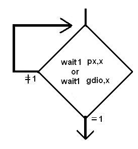
wait0,wait1: 只能針對(duì)I/O 或register “gdio”,但不能對(duì)記憶體, 其功能如流程圖所示,一直要等到I/O 或gdio.x =0 或1 成立才往下繼續(xù)執(zhí)行,因傳統(tǒng)的MCU,只有一顆MCU,故無法去實(shí)現(xiàn)這種指令,否則如果條件不成立,程式就一直停在那,形同“當(dāng)機(jī)”.
delay :直接delay x 個(gè)system clock 才往下繼續(xù)執(zhí)行, 例如system clock = 8Mhz,pmode = 0,FPP#0 執(zhí)行“delay 100” =100*1/4M = 25us,但FPPA#1執(zhí)行“delay 100” = 100 * 1/1M = 100us.
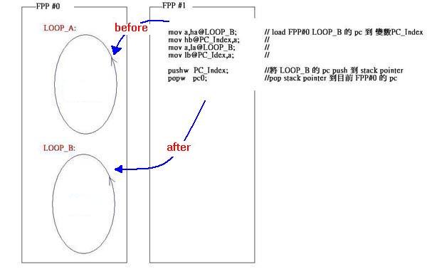
pushw,popw: push & pop 程式指標(biāo)
由于PFPA 是一顆8 核心的MCU,不同MCU 間可更改彼此的程式指標(biāo)“pc”, 來達(dá)到強(qiáng)迫其他MCU 去執(zhí)行某段程式的路徑之目的,但要小心運(yùn)用,否則容易破壞程式的結(jié)構(gòu).下例中的FPP#0 原本只會(huì)在LOOP_A無窮的回圈中打轉(zhuǎn), FPP#1 經(jīng)由“pushw” 和“popw” 改變了FPP#0 的程式指標(biāo), 讓FPP#0 變在LOOP_B無窮回圈中打轉(zhuǎn).
逐高電子技術(shù)部整理